Analysis
ESD Test
The escape of charges accumulated in objects due to friction is called Electrostatic Discharge (ESD) and ESD is an important test item that must be verified as it can cause damage to semiconductor elements.
▶ Inquiry/Request for Analysis : cs@techline.co.kr
Depending on the various situations in which a semiconductor device or element will experience actual ESD, the ESD test model is identified.
Human Body Model (HBM)
This test assumes that two objects in the state of loss of charge or gain are 'semi-conductor' and 'human body' and construct a circuit imitating the characteristics of the human body and test the semiconductor by applying ESD pulse.
Machine Model (MM)
This test simulates ESD phenomena in which electric discharge occurs when contact with other objects is made after accumulating electric charge while rubbing against equipment or nearby metals during semiconductor manufacturing process.
Charged Device Model (CDM)
It is a test simulating the most close mechanism of field defect and discharge after accumulating an electrical charge in a semiconductor package.
Various ESD test services are available in accordance with MIL, JEDEC, ANSI, IEC and AECQ specifications.
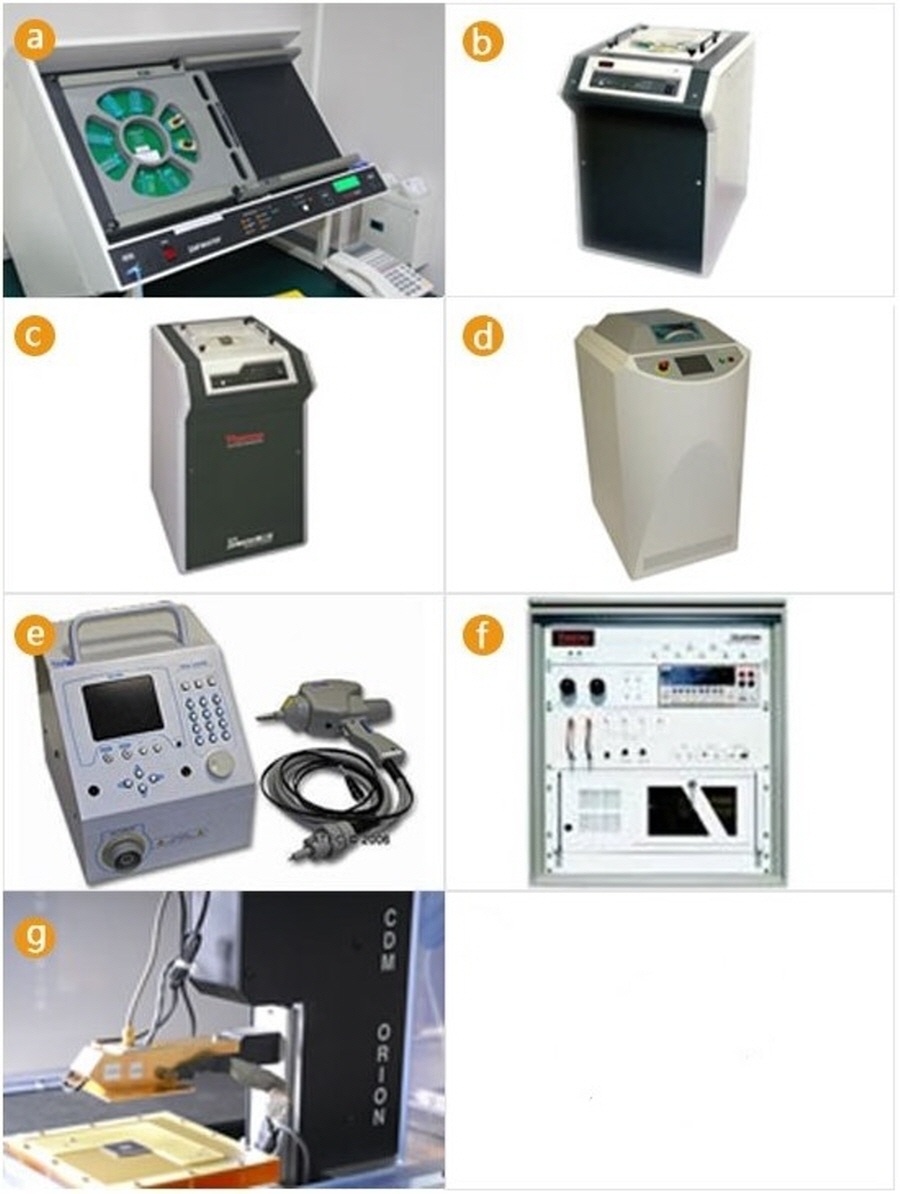
Zapmaster(a) : HBM/MM/SCDM
MK1(b) : HBM/MM/LU/HT LU
MK2(c) : HBM/MM/LU/HT LU
MK4(d) : HBM/MM/LU/HT LU/Transient-LU
ESD gun(e) : IEC/ISO/AEC
Celestron(f) : TLP
Oryx(g) : NCDMEOS
EOS (Electric Over Stress) : IEC